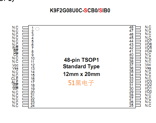
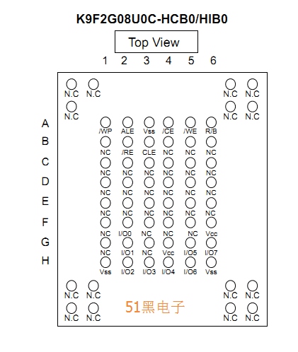
K9F2G08U0C(NAND FLASH)的引腳圖:


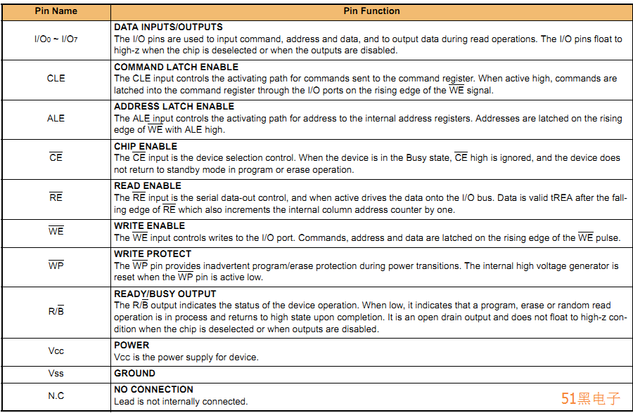
K9F2G08U0C管腳功能定義:

2.0 PRODUCT INTRODUCTION
NAND Flash Memory has addresses multiplexed into 8 I/Os. This scheme dramatically reduces pin counts and allows system upgrades to future densities
by maintaining consistency in system board design. Command, address and data are all written through I/O's by bringing WE to low while CE is low.
Those are latched on the rising edge of WE. Command Latch Enable(CLE) and Address Latch Enable(ALE) are used to multiplex command and address
respectively, via the I/O pins. Some commands require one bus cycle. For example, Reset Command, Status Read Command, etc. require just one cycle
bus. Some other commands, like page read and block erase and page program, require two cycles: one cycle for setup and the other cycle for execution..
Page Read and Page Program need the same five address cycles following the required command input. In Block Erase operation, however, only the
three row address cycles are used. Device operations are selected by writing specific commands into the command register. Table 1 defines the specific
commands of the K9G2G08U0C.
完整的pdf格式文檔51黑下載地址:
 K9F2G08U0C(NAND FLASH).pdf
(701.39 KB, 下載次數(shù): 28)
2018-11-4 21:38 上傳
點擊文件名下載附件
|
